Metrology Standard Wafer
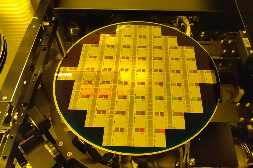
We handle standard wafers for inspection purposes.
- AOI Defect Standard Wafer (DSW)
- Step Height Standard Wafer
- XY Alignment Standard Wafer
- Overlay Standard Wafer (OVL)
- Custom Standard Wafer
We offer a variety of evaluation and calibration solutions, including defect standard wafers (DSW) for AOI (Automatic Optical Inspection) systems, step height standard wafers, and XY alignment standard wafers.
We can also accommodate customization based on your evaluation requirements and equipment specifications, such as wafer size, substrate material, defect specifications, and pattern designs.
Our standard wafers can be utilized across a wide range of fields, including research and development, equipment installation evaluation, process control, and quality assurance.
AOI Defect Standard Wafer (DSW)
The AOI Defect Standard Wafer (DSW) is a standard wafer designed for performance evaluation and calibration purposes of Automatic Optical Inspection (AOI) systems.
It features patterns that simulate various defects commonly encountered in actual semiconductor manufacturing processes, enabling its use for evaluating AOI system detection sensitivity, verifying defect detection capabilities, recipe development, and algorithm validation.
Compatible with Die-to-Die comparison methods and 3-in-3-out inspection algorithms, it is also suitable for equipment installation evaluations and performance comparisons of inspection systems.
Features
- Performance evaluation and calibration for AOI systems
- Supports Die-to-Die inspection
- Compatible with 3-in-3-out algorithms
- Equipped with Memory/Logic patterns
- Supports XY stage position calibration
- Compatible with evaluations for multiple process nodes
- Custom defect design available
Applications
- AOI system evaluation
- Equipment calibration
- Recipe development
- Algorithm validation
- Performance evaluation
Specifications
| Item | Details |
|---|---|
| Size | 6-inch, 8-inch |
| Substrate | P-type low-doped Si |
| Thickness | 725 μm |
| Packaging | Single wafer case (vacuum-packed) |
Step Height Standard Wafer
The Step Height Standard Wafer is a standard wafer designed for calibration and performance evaluation purposes of various measurement equipment such as AFM, surface profilers, white light interferometers, and 3D shape measurement devices.
Alignment patterns are formed on the wafer in both the X-axis and Y-axis directions, making it suitable for position alignment and stage accuracy evaluation.
Additionally, the central area features a highly precise step structure, which is ideal for verifying step measurement accuracy, evaluating measurement position reproducibility, and leveling adjustments.
In addition to the standard specifications, customized step heights and pattern designs can also be accommodated based on customer requirements.
Features
- Compatible with AFM, profilers, and white light interferometers
- Equipped with high-precision step patterns
- Includes XY alignment functionality
- Designed for calibration and performance evaluation of measurement devices
- Supports evaluation of measurement position reproducibility
- Customizable step height specifications available
Applications
- Evaluation of step measurement accuracy
- Calibration of measurement devices
- Performance evaluation of equipment
- Stage position accuracy evaluation
- Leveling adjustments
Specifications
| Item | Details |
|---|---|
| Size | 6-inch, 8-inch |
| Substrate | P-type low-doped Si |
| Thickness | 725 μm |
| Packaging | Single wafer case (vacuum-packed) |
XY Alignment Standard Wafer
The XY Alignment Standard Wafer is a standard wafer designed for evaluating and calibrating the position accuracy of XY stages.
It can be used with various inspection and measurement equipment such as AFM, film thickness measurement devices, SEM, and 3D shape measurement devices to verify stage position accuracy and evaluate alignment performance.
The wafer is equipped with XY stage calibration patterns that support different magnification conditions, enabling high-precision alignment and stage accuracy evaluation.
Additionally, to accommodate different recognition algorithms, two types of alignment marks, Type 1 and Type 2, are available, allowing users to select the appropriate option according to their evaluation environment.
Features
- Evaluation and calibration of XY stage position accuracy
- Equipped with high-precision alignment patterns
- Designed to support multiple magnification conditions
- Compatible with AFM, SEM, and film thickness measurement devices
- Supports Type 1 / Type 2 alignment marks
- Capable of evaluating stage position reproducibility
Applications
- XY stage calibration
- Alignment performance evaluation
- Position accuracy evaluation
- Evaluation of inspection and measurement device implementation
- Device performance evaluation
Specifications
| Item | Details |
|---|---|
| Size | 12 inches |
| Model | KG-12" XY-Type1 / KG-12" XY-Type2 |
| Substrate | P-type low-doped Si |
| Thickness | 775 μm |
| Packaging | Single wafer case (vacuum-packed) |
Overlay Standard Wafer
The OVL Standard Wafer is a standard wafer designed for evaluating and calibrating overlay accuracy in exposure systems, alignment systems, and various measurement devices.
It is equipped with OVL evaluation patterns for both same-layer and different-layer configurations, enabling the evaluation of overlay accuracy, device calibration, and validation of measurement algorithms.
Features
- Designed for overlay accuracy evaluation
- Supports Bar-in-Bar / Box-in-Box / AIM
- Compatible with same-layer and different-layer OVL evaluation
- Equipped with CD (Critical Dimension) and dimensional calibration patterns
- Includes lens distortion correction patterns
- Suitable for device calibration and performance evaluation
Applications
- Overlay accuracy evaluation
- Exposure system evaluation
- Alignment performance evaluation
- Calibration of measurement devices
- Process development
- Algorithm validation
Specifications
| Item | Details |
|---|---|
| Size | 8 inches |
| Substrate | P-type low-doped Si |
| Thickness | 725 ± 25 μm |
| Shot size | 20 × 21 mm |
| Packaging | Single wafer case (vacuum-packed) |
Calibration Patterns
- CD (Critical Dimension) and dimensional calibration patterns
- Lens distortion correction patterns
- Same-layer OVL calibration patterns
- Two-layer OVL calibration patterns
Custom Standard Wafer
We offer customization to match your evaluation conditions and equipment specifications, including defect size, defect shape, step height, alignment patterns, and wafer size.
From research and development applications to mass production equipment evaluation, we provide standard wafers tailored to a wide range of needs.
Features
- Customizable defect specifications
- Customizable step specifications
- Support for alignment pattern design
- Compatible with various wafer sizes
- Design tailored to evaluation applications
※ In addition to the products listed above, we can design and manufacture various inspection and measurement standard wafers based on your requirements. For more details, please feel free to contact us.